Schematic diagram of a dds generator on an atmel microcontroller. Functional dds generator on plc. Test of generator operating modes after assembly
Read also
Maximum frequency - 65534 Hz (and up to 8 MHz HS output with square wave). And then I thought that a generator is an excellent task where the FPGA can show itself at its best. As a matter of sport, I decided to repeat the project on FPGA, while meeting the deadlines within two weekends, and getting the parameters not strictly defined, but the maximum possible. You can find out what came out of this under the cut.
Day zero
Before the weekend arrived, I had some time to think about the implementation. To simplify my task, I decided to make the generator not as a separate device with buttons and an LCD screen, but as a device that connects to a PC via USB. For this I have a USB2RS232 board. The board does not require drivers (CDC), therefore, I think it will work under Linux (for some this is important). Also, I will not hide that I have already worked with receiving messages via RS232. I will take ready-made modules for working with RS232 from opencores.com.To generate a sine wave signal you will need a DAC. I chose the DAC type, as in the original project - R2R 8-bit. It will allow you to operate at high frequencies, on the order of megahertz. I am convinced that the FPGA should cope with this
I was thinking about how to write a program for transmitting data via a COM port. On the one hand, you can write in Delphi7; you already have experience writing such a program, and besides, the size of the executable file will not be large. I also tried to sketch out something to work with Serial in the form of a java script in an html page, but it more or less worked only through the Chrome serial API, but for this you need to install a plugin... in general, it’s also out of the question. I tried PyQt5 as an innovation for myself, but when distributing such a project, you need to drag a bunch of libraries. Having tried to compile a PyQt project into an exe file, it turned out to be more than 10 MB. That is, it will be no better than an application written in C++\Qt5. It’s also worth considering that I don’t have experience developing in python, but I do have experience in Qt5. Therefore, the choice fell on Qt5. Since the fifth version, a module for working with serial appeared and I have already worked with it. And an application based on Qt5 can be transferred to Linux and Mac (for some this is important), and from version 5.2, applications based on QWidgets can even be transferred to a smartphone!
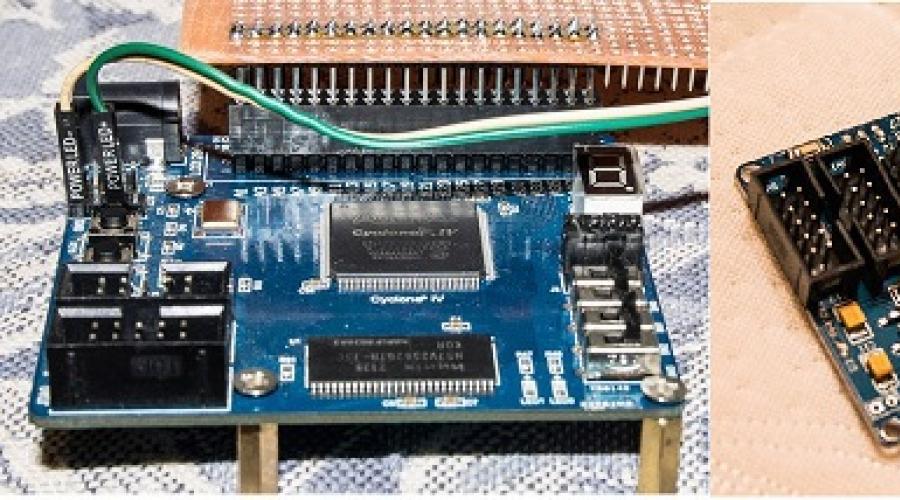
What else is needed? Naturally, the board has an FPGA. I have two of them (Cyclone iv EP4CE10E22C8N for 10 thousand cells, and Cyclone ii EP2C5 for 5 thousand cells). I'll choose the one on the left solely because of the more convenient connector. In terms of volume, the project does not intend to be large, so it will fit into either of the two. They are no different in speed. Both boards have 50 MHz oscillators on board, and inside the FPGA there is a PLL, with which I can increase the frequency to the planned 200 MHz.

The first day
Due to the fact that I had already made the DDS module in my synthesizer project, I immediately took up the soldering iron and started soldering the DAC with resistors. I took a prototype board. The installation was done using wrapping. The only change that affected the technology was that I abandoned the F38N acid for tinning the stands in favor of the TT indicator flux gel. The essence of the technology is simple: I solder racks into a printed circuit board, and solder resistors on them from the printed circuit board side. I make the missing connections by twisting. Also, the racks are convenient because I can insert them directly into the FPGA board.Unfortunately, there were no 1 and 2 kilo-ohm resistors available at home. There was no time to go to the store. I had to give up one of my rules and remove resistors from the old unnecessary board. 15K and 30K resistors were used there. The result is this Frankenstein:

After creating the project, you need to set the target device: Menu Assigments -> Device


In the project, I coded the uncontrollable main DDS module to a fixed frequency.
1000 Hz Generator Module
module signal_generator(clk50M, signal_out); input wire clk50M; wire output signal_out; wire clk200M; osc osc_200M reg accumulator; assign signal_out = accumulator; //try to generate 1000 Hz //50,000,000 Hz - clock frequency of the external generator //2^32 = 4,294,967,296 - DDS bit depth - 32 bits //divide 1000Hz / 50,000,000 Hz / 2 * 4294967296 => 42949, 67296 always @(posedge clk50M) begin accumulator<= accumulator + 32"d42949; end endmodule
After that, I clicked “Start Compilation” so that the development environment would ask what input/output lines we have in the main module of the project and what physical PINs they are connected to. You can connect to almost anyone. After compilation, we assign the lines that appear to the real PINs of the chip FPGA:
Menu item Assigments -> Pin Planner
Please ignore the HS_OUT, key0 and key1 lines for now, they appear in the project later, but I didn’t have time to take a screenshot at the very beginning.

In principle, it is enough to “register” only PIN_nn in the Location column, and the remaining parameters (I/O standard, Current Strench and Slew Rate) can be left by default, or you can select the same ones that are offered by default (default) so that there is no warning "ov.
How can I find out which PIN corresponds to the connector number on the board?
The connector pin numbers are marked on the board

And the FPGA pins to which the connector contacts are connected are described in the documentation that comes with the FPGA board.

After the pins are assigned, I compile the project again and flash it using a USB programmer. If you do not have drivers installed for the USB Byte blaster programmer, then tell Windows that they are located in the folder where you have Quartus installed. Then she will find it herself.
The programmer must be connected to the JTAG connector. And the menu item for programming is “Tools -> Programmer” (or click the icon on the toolbar). The “Start” button, the joyful “Success” and the firmware are already inside the FPGA and are already working. Just don’t turn off the FPGA, otherwise it will forget everything.
Tools -> Programmer

The DAC is connected to the FPGA board connector. I connect an oscilloscope S1-112A to the DAC output. The result should be a “saw” because the high-order part of the DDS word of the phase accumulator is output to the 8-bit output. And it always increases until it overflows.
Some 1.5 hours and for a frequency of 1000 Hz I see the following oscillogram:

I would like to note that the “saw” has a small fracture in the middle. It is due to the fact that resistors have a range of values.
Another important point that needed to be clarified is the maximum possible frequency with which the DDS generator will operate. With correctly configured TimeQuest parameters, after compilation in the “Compilation Report” you can see that the speed of the circuit is above 200 MHz with a margin. This means that I will multiply the generator frequency of 50 MHz by 4 using PLL. I will increase the value of the DDS phase accumulator with a frequency of 200 MHz. The final frequency range that can be obtained under our conditions is 0 - 100 MHz. Frequency setting accuracy:
200,000,000 Hz (clk) / 2^32 (DDS) = 0.047 Hz
That is, it is better than ~0.05 Hz. I consider the accuracy of a fraction of a hertz to be sufficient for a generator with such a range of operating frequencies (0...100 MHz). If someone needs to increase the accuracy, then for this they can increase the DDS bit depth (remember to check the TimeQuest Timing Analyzer that the operating speed of the logic circuit was within CLK = 200 MHz, since this is an adder), or simply reduce the clock frequency, if such a wide frequency range is not required.
TimeQuest Timing Analyzer

After I saw “saw” on the screen, family matters forced me to go to the country (it was my day off). There I mowed, cooked, barbecued and had no idea about the surprise that was waiting for me in the evening. Closer to night, before going to bed, I decided to look at the signal shape for other frequencies.
For frequency 100 kHz

For frequency 250 kHz

For frequency 500 kHz

For 1 MHz frequency

Second day
Due to the fact that it was interesting how the DAC would work on resistors of 100 and 200 Ohms, I immediately took up the soldering iron. This time the DAC turned out to be more accurate, and it took less time to install it.

We put the DAC on the FPGA board and connect it to the oscilloscope

Checking 1 MHz - VO! It's a completely different matter!

Saw 10 MHz

Saw 25 MHz

The shape of the 10 MHz saw is still similar to the correct one. But at 25 MHz it is no longer “pretty” at all. However, the C1-112a has a bandwidth of 10 MHz, so in this case the reason may already be in the oscilloscope.
In principle, this issue with the DAC can be considered closed. Now let's take waveforms of the high-speed output. To do this, we will output the most significant bit to a separate PIN of the FPGA. We will take the data for this line from the most significant bit of the DDS accumulator.
Assign hs_out = accumulator;
Square wave 1 MHz

Square wave 5 MHz

Square wave 25 MHz

The 50 MHz square wave is almost invisible now

But I think that the FPGA output should be loaded with resistance. Perhaps the fronts would have been steeper.
The sine is done according to the table. The table size is 256 values of 8 bits. It would have been possible to take more, but I already had a ready-made mif file. Using the wizard, we create a ROM element with sine table data from the mif file.
Creating a ROM - Tools -> Mega Wizard Plugin manager

Select 1 port ROM and give the module a name

We agree

We agree here too

Using browse, we find our mif file with the sine table

We don’t change anything here either.

Uncheck the module sine_rom_bb.v - it is not needed. Next finish. Quartus will ask you to add a module to the project - we agree. After this, the module can be used just like any other module in Verilog.

The upper 8 bits of the DDS accumulator word will be used as the ROM address, and the data output will be the sine value.
Code
//sine rom wire sine_out; sine_rom sine1(.clock(clk200M), .address(accumulator), .q(sine_out));
The oscillogram of a sine wave at different frequencies looks... the same.

If desired, you can consider DAC problems associated with resistor spread:

Well, that's the end of the weekend. But software for control from a PC has not yet been written. I am forced to admit the fact that I did not meet the planned deadlines.
Day three
There is very little time, so we write the program in a hurry (in the best traditions). In some places, in order to reduce the number of letters and the convenience of entering information from the keyboard, an event filter is used by the widget name. Please understand and forgive.Interface

Links with analogues
Not a complete listFunctional DDS generator. Created based on AVR. Frequencies 0... 65534 Hz.
Review of DDS generator GK101. Created using Altera MAX240 FPGA. Frequencies up to 10 MHz.
Multifunction generator on PIC16F870. Frequency range: 11 Hz - 60 kHz.
generators Add tags
Maximum frequency - 65534 Hz (and up to 8 MHz HS output with square wave). And then I thought that a generator is an excellent task where the FPGA can show itself at its best. As a matter of sport, I decided to repeat the project on FPGA, while meeting the deadlines within two weekends, and getting the parameters not strictly defined, but the maximum possible. You can find out what came out of this under the cut.
Day zero
Before the weekend arrived, I had some time to think about the implementation. To simplify my task, I decided to make the generator not as a separate device with buttons and an LCD screen, but as a device that connects to a PC via USB. For this I have a USB2RS232 board. The board does not require drivers (CDC), therefore, I think it will work under Linux (for some this is important). Also, I will not hide that I have already worked with receiving messages via RS232. I will take ready-made modules for working with RS232 from opencores.com.To generate a sine wave signal you will need a DAC. I chose the DAC type, as in the original project - R2R 8-bit. It will allow you to operate at high frequencies, on the order of megahertz. I am convinced that the FPGA should cope with this
I was thinking about how to write a program for transmitting data via a COM port. On the one hand, you can write in Delphi7; you already have experience writing such a program, and besides, the size of the executable file will not be large. I also tried to sketch out something to work with Serial in the form of a java script in an html page, but it more or less worked only through the Chrome serial API, but for this you need to install a plugin... in general, it’s also out of the question. I tried PyQt5 as an innovation for myself, but when distributing such a project, you need to drag a bunch of libraries. Having tried to compile a PyQt project into an exe file, it turned out to be more than 10 MB. That is, it will be no better than an application written in C++\Qt5. It’s also worth considering that I don’t have experience developing in python, but I do have experience in Qt5. Therefore, the choice fell on Qt5. Since the fifth version, a module for working with serial appeared and I have already worked with it. And an application based on Qt5 can be transferred to Linux and Mac (for some this is important), and from version 5.2, applications based on QWidgets can even be transferred to a smartphone!
What else is needed? Naturally, the board has an FPGA. I have two of them (Cyclone iv EP4CE10E22C8N for 10 thousand cells, and Cyclone ii EP2C5 for 5 thousand cells). I'll choose the one on the left solely because of the more convenient connector. In terms of volume, the project does not intend to be large, so it will fit into either of the two. They are no different in speed. Both boards have 50 MHz oscillators on board, and inside the FPGA there is a PLL, with which I can increase the frequency to the planned 200 MHz.
The first day
Due to the fact that I had already made the DDS module in my synthesizer project, I immediately took up the soldering iron and started soldering the DAC with resistors. I took a prototype board. Installation was done using . The only change that affected the technology was that I abandoned the F38N acid for tinning the stands in favor of the TT indicator flux gel. The essence of the technology is simple: I solder racks into a printed circuit board, and solder resistors on them from the printed circuit board side. I make the missing connections by twisting. Also, the racks are convenient because I can insert them directly into the FPGA board.Unfortunately, there were no 1 and 2 kilo-ohm resistors available at home. There was no time to go to the store. I had to give up one of my rules and remove resistors from the old unnecessary board. 15K and 30K resistors were used there. The result is this Frankenstein:
After creating the project, you need to set the target device: Menu Assigments -> Device
In the project, I coded the uncontrollable main DDS module to a fixed frequency.
1000 Hz Generator Module
module signal_generator(clk50M, signal_out); input wire clk50M; wire output signal_out; wire clk200M; osc osc_200M reg accumulator; assign signal_out = accumulator; //try to generate 1000 Hz //50,000,000 Hz - clock frequency of the external generator //2^32 = 4,294,967,296 - DDS bit depth - 32 bits //divide 1000Hz / 50,000,000 Hz / 2 * 4294967296 => 42949, 67296 always @(posedge clk50M) begin accumulator<= accumulator + 32"d42949; end endmodule
After that, I clicked “Start Compilation” so that the development environment would ask what input/output lines we have in the main module of the project and what physical PINs they are connected to. You can connect to almost anyone. After compilation, we assign the lines that appear to the real PINs of the chip FPGA:
Menu item Assigments -> Pin Planner
Please ignore the HS_OUT, key0 and key1 lines for now, they appear in the project later, but I didn’t have time to take a screenshot at the very beginning.
In principle, it is enough to “register” only PIN_nn in the Location column, and the remaining parameters (I/O standard, Current Strench and Slew Rate) can be left by default, or you can select the same ones that are offered by default (default) so that there is no warning "ov.
How can I find out which PIN corresponds to the connector number on the board?
The connector pin numbers are marked on the board
And the FPGA pins to which the connector contacts are connected are described in the documentation that comes with the FPGA board.
After the pins are assigned, I compile the project again and flash it using a USB programmer. If you do not have drivers installed for the USB Byte blaster programmer, then tell Windows that they are located in the folder where you have Quartus installed. Then she will find it herself.
The programmer must be connected to the JTAG connector. And the menu item for programming is “Tools -> Programmer” (or click the icon on the toolbar). The “Start” button, the joyful “Success” and the firmware are already inside the FPGA and are already working. Just don’t turn off the FPGA, otherwise it will forget everything.
Tools -> Programmer
The DAC is connected to the FPGA board connector. I connect an oscilloscope S1-112A to the DAC output. The result should be a “saw” because the high-order part of the DDS word of the phase accumulator is output to the 8-bit output. And it always increases until it overflows.
Some 1.5 hours and for a frequency of 1000 Hz I see the following oscillogram:
I would like to note that the “saw” has a small fracture in the middle. It is due to the fact that resistors have a range of values.
Another important point that needed to be clarified is the maximum possible frequency with which the DDS generator will operate. With correctly configured TimeQuest parameters, after compilation in the “Compilation Report” you can see that the speed of the circuit is above 200 MHz with a margin. This means that I will multiply the generator frequency of 50 MHz by 4 using PLL. I will increase the value of the DDS phase accumulator with a frequency of 200 MHz. The final frequency range that can be obtained under our conditions is 0 - 100 MHz. Frequency setting accuracy:
200,000,000 Hz (clk) / 2^32 (DDS) = 0.047 Hz
That is, it is better than ~0.05 Hz. I consider the accuracy of a fraction of a hertz to be sufficient for a generator with such a range of operating frequencies (0...100 MHz). If someone needs to increase the accuracy, then for this they can increase the DDS bit depth (remember to check the TimeQuest Timing Analyzer that the operating speed of the logic circuit was within CLK = 200 MHz, since this is an adder), or simply reduce the clock frequency, if such a wide frequency range is not required.
TimeQuest Timing Analyzer
After I saw “saw” on the screen, family matters forced me to go to the country (it was my day off). There I mowed, cooked, barbecued and had no idea about the surprise that was waiting for me in the evening. Closer to night, before going to bed, I decided to look at the signal shape for other frequencies.
For frequency 100 kHz
For frequency 250 kHz
For frequency 500 kHz
For 1 MHz frequency
Second day
Due to the fact that it was interesting how the DAC would work on resistors of 100 and 200 Ohms, I immediately took up the soldering iron. This time the DAC turned out to be more accurate, and it took less time to install it.
We put the DAC on the FPGA board and connect it to the oscilloscope
Checking 1 MHz - VO! It's a completely different matter!
Saw 10 MHz
Saw 25 MHz
The shape of the 10 MHz saw is still similar to the correct one. But at 25 MHz it is no longer “pretty” at all. However, the C1-112a has a bandwidth of 10 MHz, so in this case the reason may already be in the oscilloscope.
In principle, this issue with the DAC can be considered closed. Now let's take waveforms of the high-speed output. To do this, we will output the most significant bit to a separate PIN of the FPGA. We will take the data for this line from the most significant bit of the DDS accumulator.
Assign hs_out = accumulator;
Square wave 1 MHz
Square wave 5 MHz
Square wave 25 MHz
The 50 MHz square wave is almost invisible now
But I think that the FPGA output should be loaded with resistance. Perhaps the fronts would have been steeper.
The sine is done according to the table. The table size is 256 values of 8 bits. It would have been possible to take more, but I already had a ready-made mif file. Using the wizard, we create a ROM element with sine table data from the mif file.
Creating a ROM - Tools -> Mega Wizard Plugin manager
Select 1 port ROM and give the module a name
We agree
We agree here too
Using browse, we find our mif file with the sine table
We don’t change anything here either.
Uncheck the module sine_rom_bb.v - it is not needed. Next finish. Quartus will ask you to add a module to the project - we agree. After this, the module can be used just like any other module in Verilog.
The upper 8 bits of the DDS accumulator word will be used as the ROM address, and the data output will be the sine value.
Code
//sine rom wire sine_out; sine_rom sine1(.clock(clk200M), .address(accumulator), .q(sine_out));
The oscillogram of a sine wave at different frequencies looks... the same.
If desired, you can consider DAC problems associated with resistor spread:
Well, that's the end of the weekend. But software for control from a PC has not yet been written. I am forced to admit the fact that I did not meet the planned deadlines.
Day three
There is very little time, so we write the program in a hurry (in the best traditions). In some places, in order to reduce the number of letters and the convenience of entering information from the keyboard, an event filter is used by the widget name. Please understand and forgive.Interface
Links with analogues
Not a complete listFunctional DDS generator. Created based on AVR. Frequencies 0... 65534 Hz.
Review of DDS generator GK101. Created using Altera MAX240 FPGA. Frequencies up to 10 MHz.
Multifunction generator on PIC16F870. Frequency range: 11 Hz - 60 kHz.
generators
Any home workshop should have the necessary set of tools and measuring instruments. For people involved in amateur radio as a hobby, the high monetary costs of purchasing the necessary equipment are often unacceptable.
So in my case, the list of this equipment was far from complete and lacked signal generator.
Signal generator It turned out to be easy to make yourself from available radio elements and not expensive in the end. So, after rummaging on the Internet, I found a large number of circuits for various generators, including more advanced models with a DAC, but already expensive to manufacture. To begin with, I stopped at a simple DDS signal generator on the ATMEGA8 microcontroller from Atmel. This one, I didn’t improve or change anything - I left everything as is, I just created a copy and, especially, I don’t claim the authorship of this device.
So, signal generator has good characteristics and is suitable for solving simple problems.
Displaying information in signal generator produced on a 16x2 character LCD display with an HD44780 controller. It is noteworthy that to save microcontroller ports, the LCD display is controlled via only three wires; this was achieved by using a shift register - read about how to connect a display via three wires.
Saving ports is necessary, 8 ports are used for a resistive DAC, 7 ports for buttons. In the original article, the author promised to use PWM modulation, but apparently did not finish it, since he began developing a more advanced version on ATMEGA16.
Schematic diagram of a DDS signal generator and printed circuit board.
The circuit and boards are shown in the original; they also contain buttons for PWM control not used by the author.
For the DAC, I specifically bought precision resistors with an error of ±0.05%, but as it turned out, simple ones with an error of ±5% are quite sufficient. The signal shape was quite acceptable for all types of signals.
When generator assembled and the program loaded into the microcontroller, no settings are required, unless you adjust the display contrast.
Working with the device is simple - select the signal shape, set the required frequency, and you can change the frequency setting step with limits of 1 - 10 - 100 - 1000 Hz per step. Then click on Start and the generator starts working. It should be noted that when the generator is started, the frequency and shape of the signal cannot be changed, this is due to the fact that the program goes into an endless loop and in order to increase the maximum generation frequency, the button polling procedure had to be removed. To stop generation, click on stop/reset, this restarts the program and it returns to the settings menu. Here's the nuance.
Separately, I would like to tell you about the manufacture of the housing for the generator. You can purchase a ready-made case in a store or use a suitable one from some other device, but I decided to make it entirely myself. A piece of double-sided fiberglass lay idle, which I donated to the body.
First, you need to take all the measurements, the dimensions of the LCD display and signal generator board, power supply, connectors and buttons, then place it on a sheet of paper as it will be inside the case. Based on the dimensions obtained, you can begin manufacturing.
This project is a high-quality and universal function generator, which, despite some complexity of the circuit, at least in comparison with simpler ones, has very wide functionality, which justifies the cost of its assembly. It is capable of producing 9 different waveforms and also works with pulse synchronization.
Schematic diagram of the generator on the MK

Device settings
- Frequency range: 10 Hz - 60 kHz
- Digital frequency adjustment in 3 different steps
- Waveforms: Sine, Triangle, Square, Saw, H-pulse, L-pulse, Burst, Sweep, Noise
- Output range: 15V for sine and triangle, 0-5V for other modes
- There is an output for pulse synchronization

The device is powered from 12 volts AC, which provides a sufficiently high (over 18 V) DC voltage necessary for normal operation of the 78L15 and 79L15, which form a bipolar 15 V circuit. This is done so that the LF353 microcircuit can output the full range of signals to the load 1 kOhm.

Level controller used ALPS SRBM1L0800. The circuit should use resistors with ±1% tolerance or better. LED current limiters - 4306R series resistors. Brightness can be increased depending on the preference of the performer. The generator is assembled in a plastic case 178x154x36 mm with aluminum front and rear panels.

Many contact components are mounted on the front and rear panels (buttons, knobs, RCA connectors, LED assemblies, power connector). Printed circuit boards are attached to the housing with bolts with plastic spacers. All other elements of the generator are mounted on printed circuit boards - the power supply is separate. The left button in the middle is to change the mode, the right one is to select the mode frequency.

The generator produces various signals and operates in three modes, which are selected using the "Select" key and indicated by the three upper (in the diagram) LEDs. The rotary control changes the signal parameters according to the following table:

Immediately after setting in mode 1, sine generation occurs. However, the starting frequency is quite low and at least one click of the encoder is needed to increase it. The board has a contact for connecting the device for programming, which allows you to quickly change the functionality of the signal generator, if necessary. All project files - PIC16F870 firmware, board drawings, are located
This DDS function generator (version 2.0) of signals is assembled on an AVR microcontroller, has good functionality, has amplitude control, and is also assembled on a single-sided printed circuit board.
This generator is based on the Jesper DDS generator algorithm, the program has been modernized for AVR-GCC C with assembly code inserts. The generator has two output signals: the first is DDS signals, the second is a high-speed (1..8 MHz) “rectangular” output, which can be used to revive the MK with incorrect fuzzes and for other purposes.
The high-speed HS (High Speed) signal is taken directly from the Atmega16 OC1A (PD5) microcontroller.
DDS signals are generated from other MC outputs through a resistive R2R matrix and through the LM358N chip, which allows adjustment of the signal amplitude and offset. Offset and amplitude are adjusted using two potentiometers. The offset can be adjusted in the range of +5V..-5V, and the amplitude is 0...10V. The frequency of DDS signals can be adjusted within the range of 0... 65534 Hz, this is more than enough for testing audio circuits and other amateur radio tasks.
Main characteristics of DDS generator V2.0:
- a simple circuit with common and inexpensive radioelements;
- single-sided printed circuit board;
- built-in power supply;
- separate high-speed output (HS) up to 8 MHz;
- DDS signals with variable amplitude and offset;
- DDS signals: sine, rectangle, saw and reverse saw, triangle, ECG signal and noise signal;
- 2×16 LCD screen;
- intuitive 5-button keyboard;
- steps for frequency adjustment: 1, 10, 100, 1000, 10000 Hz;
- remembering the last state after turning on the power.
The block diagram below shows the logical structure of a function generator:

As you can see, the device requires several supply voltages: +5V, -12V, +12V. Voltages +12V and -12V are used to regulate signal amplitude and offset. The power supply is designed using a transformer and several voltage stabilizer chips:

The power supply is assembled on a separate board:

If you don’t want to assemble the power supply yourself, you can use a regular ATX power supply from a computer, where all the necessary voltages are already present. ATX connector layout.
LCD screen
All actions are displayed via an LCD screen. The generator is controlled by five keys

The up/down keys are used to move through the menu, the left/right keys are used to change the frequency value. When the center key is pressed, the selected signal begins to be generated. Pressing the key again stops the generator.
A separate value is provided to set the frequency change step. This is convenient if you need to change the frequency over a wide range.
The noise generator does not have any settings. It uses the usual rand() function, which is continuously fed to the output of the DDS generator.
The HS high speed output has 4 frequency modes: 1, 2, 4 and 8 MHz.
Schematic diagram
The function generator circuit is simple and contains easily accessible elements:
- AVR Atmega16 microcontroller, with external quartz at 16 MHz;
- standard HD44780-type LCD screen 2×16;
- R2R DAC matrix made of ordinary resistors;
- operational amplifier LM358N (domestic analogue of KR1040UD1);
- two potentiometers;
- five keys;
- several connectors.

Pay:
The functional generator is assembled in a plastic box: 

Software
As I said above, I based my program on the Jesper DDS generator algorithm. I added a few lines of assembly code to implement the generation stop. Now the algorithm contains 10 CPU cycles, instead of 9.
void static inline Signal_OUT(const uint8_t *signal, uint8_t ad2, uint8_t ad1, uint8_t ad0)(
asm volatile("eor r18, r18 ;r18<-0″ "\n\t"
"eor r19, r19 ;r19<-0″ "\n\t"
"1:" "\n\t"
"add r18, %0 ;1 cycle" "\n\t"
"adc r19, %1 ;1 cycle" "\n\t"
"adc %A3, %2 ;1 cycle" "\n\t"
"lpm ;3 cycles" "\n\t"
"out %4, __tmp_reg__ ;1 cycle" "\n\t"
"sbis %5, 2 ;1 cycle if no skip" "\n\t"
"rjmp 1b ;2 cycles. Total 10 cycles" "\n\t"
:
:"r" (ad0),,"r" (ad1),,"r" (ad2),,"e" (signal),,"I" (_SFR_IO_ADDR(PORTA)), "I" (_SFR_IO_ADDR(SPCR))
:"r18″, "r19″
);}
The table of DDS signal forms is located in the flash memory of the MK, the address of which starts at 0xXX00. These sections are defined in the makefile, in the appropriate memory locations:
#Define sections where to store signal tables
LDFLAGS += -Wl,-section-start=.MySection1=0x3A00
LDFLAGS += -Wl,-section-start=.MySection2=0x3B00
LDFLAGS += -Wl,-section-start=.MySection3=0x3C00
LDFLAGS += -Wl,-section-start=.MySection4=0x3D00
LDFLAGS += -Wl,-section-start=.MySection5=0x3E00
LDFLAGS += -Wl,-section-start=.MySection6=0x3F00